- 您现在的位置:买卖IC网 > Sheet目录337 > LE25S40MB-AH (ON Semiconductor)IC MEM 4MBIT SERIAL FLASH 8SOP
�� �
�
�LE25S40MB�
�BP0,� BP1,� BP2,� TB� (Bits� 2,� 3,� 4,� 5)�
�Block� protect� BP0,� BP1,� BP2� and� TB� are� status� register� bits� that� can� be� rewritten,� and� the� memory� space� to� be� protected�
�can� be� set� depending� on� these� bits.� For� the� setting� conditions,� refer� to� "Table� 5� Protect� level� setting� conditions".�
�BP0,� BP1,� and� BP2� are� used� to� select� the� protected� area� and� TB� to� allocate� the� protected� area� to� the� higher-order�
�address� area� or� lower-order� address� area.�
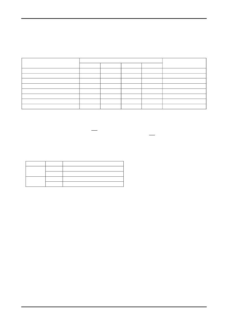
�Table� 5� Protect� Level� Setting� Conditions�
�Status� Register� Bits�
�Protect� Level�
�0� (Whole� area� unprotected)�
�T1� (Upper� side� 1/8� protected)�
�T2� (Upper� side� 1/4� protected)�
�T3� (Upper� side� 1/2� protected)�
�B1� (Lower� side� 1/8� protected)�
�B2� (Lower� side� 1/4� protected)�
�B3� (Lower� side� 1/2� protected)�
�4� (Whole� area� protected)�
�TB�
�X�
�0�
�0�
�0�
�1�
�1�
�1�
�X�
�BP2�
�0�
�0�
�0�
�0�
�1�
�1�
�1�
�1�
�BP1�
�0�
�0�
�1�
�1�
�0�
�1�
�1�
�X�
�BP0�
�0�
�1�
�0�
�1�
�1�
�0�
�1�
�X�
�Protected� Area�
�None�
�07FFFFh� to� 070000h�
�07FFFFh� to� 060000h�
�07FFFFh� to� 040000h�
�00FFFFh� to� 000000h�
�01FFFFh� to� 000000h�
�03FFFFh� to� 000000h�
�07FFFFh� to� 000000h�
�*� Chip� erase� is� enabled� only� when� the� protect� level� is� 0.�
�SRWP� (bit� 7)�
�Status� register� write� protect� SRWP� is� the� bit� for� protecting� the� status� registers,� and� its� information� can� be� rewritten.�
�When� SRWP� is� "1"� and� the� logic� level� of� the� WP� pin� is� low,� the� status� register� write� command� is� ignored,� and� status�
�registers� BP0,� BP1,� BP2,� TB� and� SRWP� are� protected.� When� the� logic� level� of� the� WP� pin� is� high,� the� status� registers�
�are� not� protected� regardless� of� the� SRWP� state.� The� SRWP� setting� conditions� are� shown� in� "Table� 6� SRWP� setting�
�conditions".�
�Table� 6� SRWP� Setting� Conditions�
�WP� Pin�
�0�
�1�
�SRWP�
�0�
�1�
�0�
�1�
�Status� Register� Protect� State�
�Unprotected�
�Protected�
�Unprotected�
�Unprotected�
�Bit� 6� are� reserved� bits,� and� have� no� significance.�
�3.� Write� Enable�
�Before� performing� any� of� the� operations� listed� below,� the� device� must� be� placed� in� the� write� enable� state.� Operation� is�
�the� same� as� for� setting� status� register� WEN� to� "1",� and� the� state� is� enabled� by� inputting� the� write� enable� command.�
�"Figure� 7� Write� Enable"� shows� the� timing� waveforms� when� the� write� enable� operation� is� performed.� The� write� enable�
�command� consists� only� of� the� first� bus� cycle,� and� it� is� initiated� by� inputting� (06h).�
�?� Small� sector� erase,� sector� erase,� chip� erase�
�?� Page� program�
�?� Status� register� write�
�No.A2096-9/22�
�发布紧急采购,3分钟左右您将得到回复。
相关PDF资料
LE25U20AMB-AH
IC MEM 2MBIT SERIAL FLASH 8SOP
LFDAS12XSIT
HARDWARE MC9S12XS 112-PIN
LFXP10E-L-EV
BOARD EVAL LATTICEXP10E STD
LH28F008SCHT-TE
IC FLASH 8MBIT 85NS 40TSOP
LH28F160S3HNS-TV
IC FLASH 16MBIT 100NS 56SSOP
LH28F160S5HNS-S1
IC FLASH 16MBIT 70NS 56SSOP
LH28F320S3HNS-ZM
IC FLASH 32MBIT 110NS 56SSOP
LH28F320SKTD-ZR
IC FLASH 32MBIT 70NS 48TSOP
相关代理商/技术参数
LE25S40QES00-AH
制造商:ON Semiconductor 功能描述:S-FLASH MEMORY(4M) - Tape and Reel
LE25S67EKS-GD0000
制造商:Legacy Electronics Inc 功能描述:512MB PC2-5300 CL5 DIMM - Bulk
LE25S80MB-AH
制造商:ON Semiconductor 功能描述:8M BIT SERIAL FLASH MEMOR - Tape and Reel 制造商:ON Semiconductor 功能描述:Flash 制造商:ON Semiconductor 功能描述:REEL - 8M BIT SERIAL FLASH MEMOR
LE25S81MCTWG
制造商:ON Semiconductor 功能描述:8M BIT SERIAL FLASH MEMOR - Tape and Reel 制造商:ON Semiconductor 功能描述:REEL - 8M BIT SERIAL FLASH MEMOR
LE25SS53DKE-CAR
制造商:Legacy Electronics Inc 功能描述:512MB PC2-4200 (533 MHZ) CL4-4-4,200 PIN SODIMM GOLD 1.181" - Bulk
LE25U20AMB
制造商:SANYO 制造商全称:Sanyo Semicon Device 功能描述:2M-bit (256K??8) Serial Flash Memory
LE25U20AMB-AH
功能描述:闪存 S-FLASH MEMORY(2M)
RoHS:否 制造商:ON Semiconductor 数据总线宽度:1 bit 存储类型:Flash 存储容量:2 MB 结构:256 K x 8 定时类型: 接口类型:SPI 访问时间: 电源电压-最大:3.6 V 电源电压-最小:2.3 V 最大工作电流:15 mA 工作温度:- 40 C to + 85 C 安装风格:SMD/SMT 封装 / 箱体: 封装:Reel
LE25U20AMBM02-AH
功能描述:闪存 RoHS:否 制造商:ON Semiconductor 数据总线宽度:1 bit 存储类型:Flash 存储容量:2 MB 结构:256 K x 8 定时类型: 接口类型:SPI 访问时间: 电源电压-最大:3.6 V 电源电压-最小:2.3 V 最大工作电流:15 mA 工作温度:- 40 C to + 85 C 安装风格:SMD/SMT 封装 / 箱体: 封装:Reel